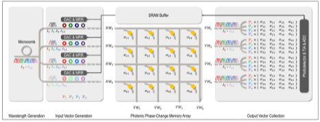
The growing computational demands of deep learning have driven interest in analog neural networks using resistive memory and silicon photonics. However, these technologies face inherent limitations in computing parallelism when used independently. Photonic phase-change memory (PCM), which integrates photonics with PCM, overcomes these constraints by enabling simultaneous processing of multiple inputs encoded on different wavelengths, significantly enhancing parallel computation for deep neural network (DNN) inference and training. This paper presents MERIT, a sustainable DNN accelerator that capitalizes on the non-volatility of resistive memory and the high operating speed of photonic devices. MERIT enables seamless inference and training by loading weight kernels into photonic PCM arrays and selectively supplying light encoded with input features for the forward pass and loss gradients for the backward pass. We compare MERIT with state-of-the-art digital and analog DNN accelerators including TPU, DEAP, and PTC. Simulation results demonstrate that MERIT reduces execution time by 68% and energy consumption by 64% for inference, and reduces execution time by 79% and energy consumption by 84% for training.
In pursuit of higher inference accuracy, deep neural network (DNN) models have significantly increased in complexity and size. To overcome the consequent computational challenges, scalable chiplet-based accelerators have been proposed. However, data communication using metallic-based interconnects in these chiplet-based DNN accelerators is becoming a primary obstacle to performance, energy efficiency, and scalability. The photonic interconnects can provide adequate data communication support due to some superior properties like low latency, high bandwidth and energy efficiency, and ease of broadcast communication. In this project, we propose SPACX: a Silicon Photonics-based Chiplet Accelerator for DNN inference applications. Specifically, SPACX includes a photonic network design that enables seamless single-chiplet and cross-chiplet broadcast communications, and a tailored dataflow that promotes data broadcast and maximizes parallelism. Furthermore, we explore the broadcast granularities of the photonic network and implications on system performance and energy efficiency. A flexible bandwidth allocation scheme is also proposed to dynamically adjust communication bandwidths for different types of data. Simulation results using several DNN models show that SPACX can achieve 78 percent and 75 percent reduction in execution time and energy, respectively, as compared to other state-of-the-art chiplet-based DNN accelerators.
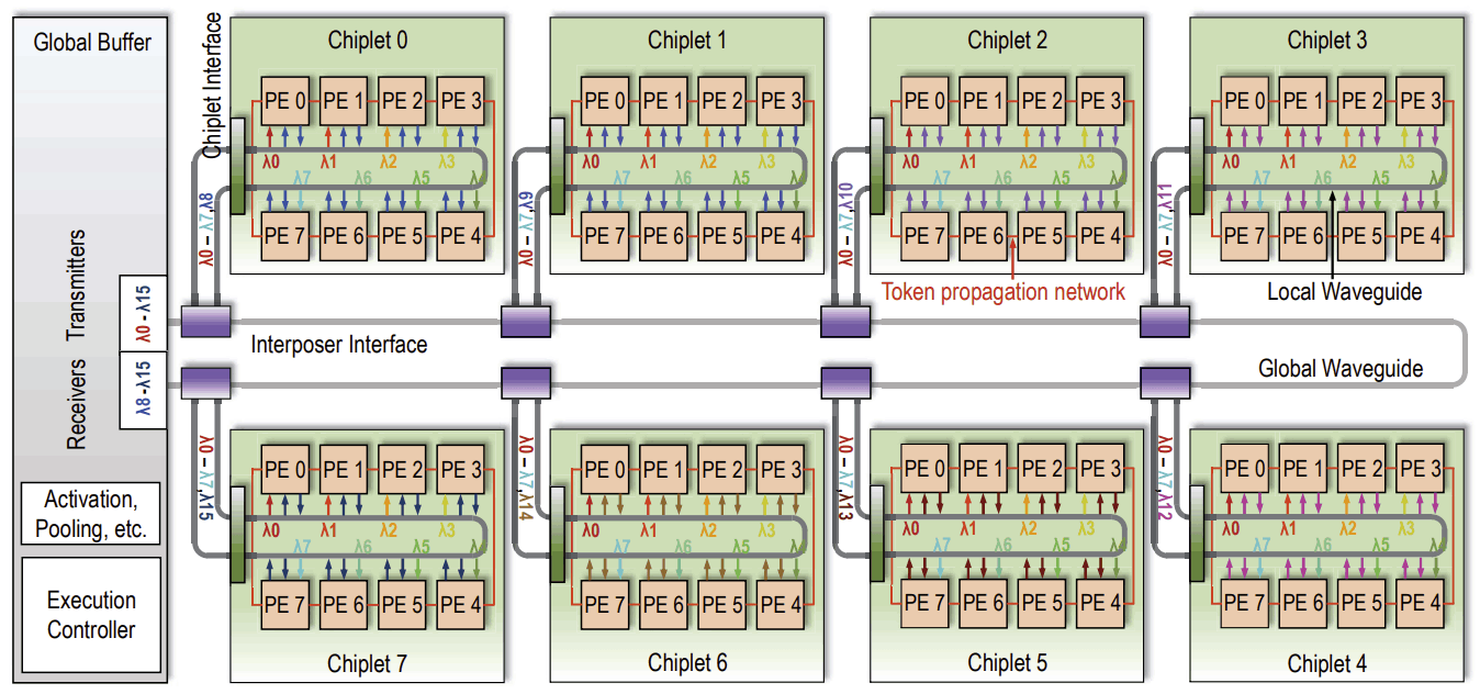
Chiplet-based convolution neural network (CNN) accelerators have emerged as a promising solution to provide substantial processing power and on-chip memory capacity for CNN inference. The performance of these accelerators is often limited by inter-chiplet metallic interconnects. Emerging technologies such as photonic interconnects can overcome the limitations of metallic interconnects due to several superior properties including high bandwidth density and distance-independent latency. However, implementing photonic interconnects in chiplet-based CNN accelerators is challenging and requires combined effort of network architectural optimization and CNN dataflow customization. In this project, we propose SPRINT, a chiplet-based CNN accelerator that consists of a global buffer and several accelerator chiplets. SPRINT introduces two novel designs: (1) a photonic inter-chiplet network that can adapt to specific communication patterns in CNN inference through wavelength allocation and waveguide reconfiguration, and (2) a CNN dataflow that can leverage the broadcasting capability of photonic interconnects while minimizing the costly electrical-to-optical and optical-to-electrical signal conversions. Simulations using multiple CNN models show that SPRINT achieves up to 76 percent and 68 percent reduction in execution time and energy consumption, respectively, as compared to other state-of-the-art chiplet-based architectures with either metallic or photonic interconnects.
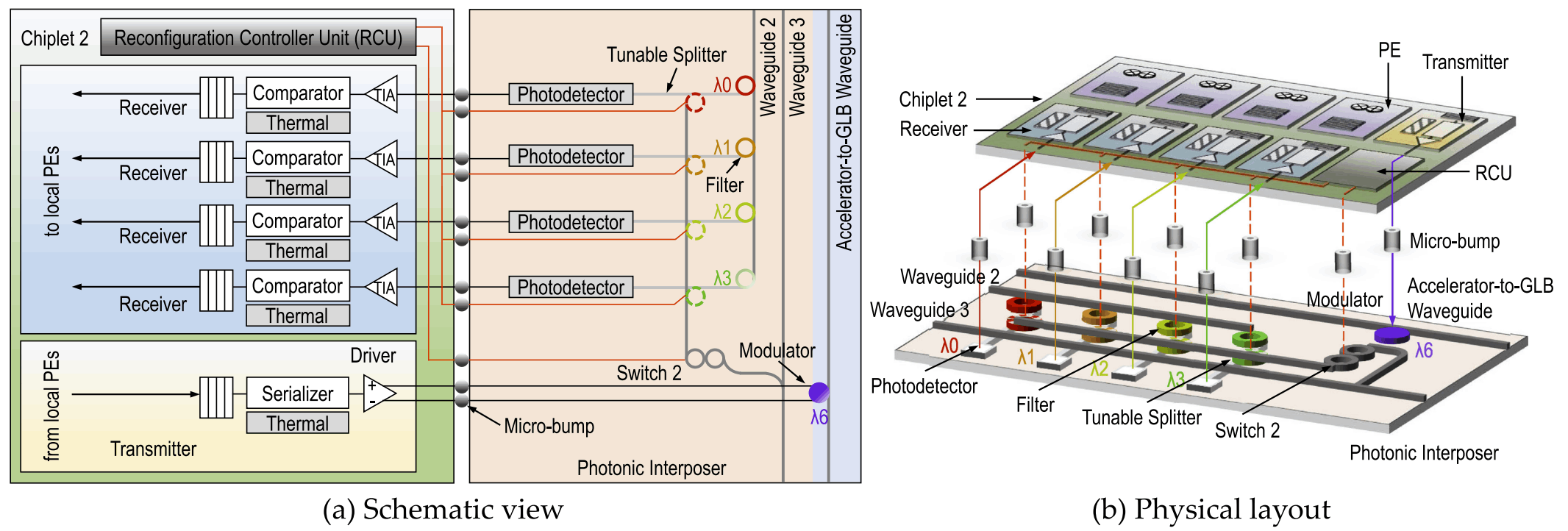
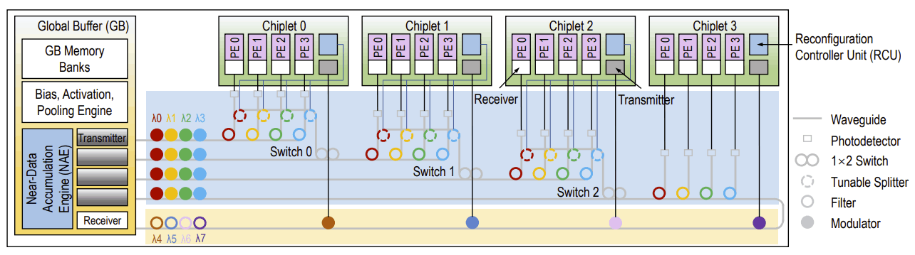
Chiplet-based architectures have been proposed to scale computing systems for deep neural networks (DNNs). Prior work has shown that for the chiplet-based DNN accelerators, the electrical network connecting the chiplets poses a major challenge to system performance, energy consumption, and scalability. Some emerging interconnect technologies such as silicon photonics can potentially overcome the challenges facing electrical interconnects as photonic interconnects provide high bandwidth density, superior energy efficiency, and ease of implementing broadcast and multicast operations that are prevalent in DNN inference. In this project, we propose a chiplet-based architecture named SPRINT for DNN inference. SPRINT uses a global buffer to simplify the data transmission between storage and computation, and includes two novel designs: (1) a reconfigurable photonic network that can support diverse communications in DN inference with minimal implementation cost, and (2) a customized dataflow that exploits the ease of broadcast and multicast feature of photonic interconnects to support highly parallel DNN computations. Simulation studies using ResNet-50 DNN model show that SPRNT achieves 46 percent and 61 percent execution time and energy consumption reduction, respectively, as compared to other state-of-the-art chiplet-based architectures with electrical or photonic interconnects.
As communication energy exceeds computation energy in future technologies, traditional on-chip electrical interconnects face fundamental challenges in the many-core era. Photonic interconnects have been proposed as a disruptive technology solution due to superior performance per Watt, distance independent energy consumption and CMOS compatibility for on-chip interconnects. Static power due to the laser being always switched on, varying link utilization due to spatial and temporal traffic fluctuations and thermal sensitivity are some of the critical challenges facing photonics interconnects. In this paper, we propose photonic interconnects for heterogeneous multicores using a checkerboard pattern that clusters CPU-GPU cores together and implements bandwidth reconfiguration using local router information without global coordination. To reduce the static power, we also propose a dynamic laser scaling technique that predicts the power level for the next epoch using the buffer occupancy of previous epoch. To further improve power-performance trade-offs, we also propose a regression-based machine learning technique for scaling the power of the photonic link. Our simulation results demonstrate a 34% performance improvement over a baseline electrical CMESH while consuming 25% less energy per bit when dynamically reallocating bandwidth. When dynamically scaling laser power, our buffer-based reactive and ML-based proactive prediction techniques show 40 - 65% in power savings with 0 - 14% in throughput loss depending on the reservation window size.
As communication energy exceeds computation energy in future technologies, traditional on-chip electrical interconnects face fundamental challenges in the many-core era. Photonic interconnects have been proposed as a disruptive technology solution due to superior performance per Watt, distance independent energy consumption and CMOS compatibility for on-chip interconnects. Static power due to the laser being always switched on, varying link utilization due to spatial and temporal traffic fluctuations and thermal sensitivity are some of the critical challenges facing photonics interconnects. In this paper, we propose photonic interconnects for heterogeneous multicores using a checkerboard pattern that clusters CPU-GPU cores together and implements bandwidth reconfiguration using local router information without global coordination. To reduce the static power, we also propose a dynamic laser scaling technique that predicts the power level for the next epoch using the buffer occupancy of previous epoch. To further improve power-performance trade-offs, we also propose a regression-based machine learning technique for scaling the power of the photonic link. Our simulation results demonstrate a 34% performance improvement over a baseline electrical CMESH while consuming 25% less energy per bit when dynamically reallocating bandwidth. When dynamically scaling laser power, our buffer-based reactive and ML-based proactive prediction techniques show 40 - 65% in power savings with 0 - 14% in throughput loss depending on the reservation window size.
As technology scales, hundreds and thousands of cores are being integrated on a single chip. Since metallic interconnects may not scale effectively to support thousands of cores, architects have proposed emerging technologies such as photonics and wireless for intra-chip communication. While photonics technology is limited by the complexity and thermal effects, wireless technology for on-chip communication is limited by the available bandwidth. In this paper, we combine the benefits of both technologies into novel architecture that takes advantage of the communication benefits of both technologies while circumventing their limits. We discuss the scalability of the proposed architecture to kilo-core system using wireless technology. We evaluate the power consumption, throughput and latency for 256 and 1024 core architectures when compared to photonics-only, wireless-wired, wireless-photonics and wired-only architectures on synthetic traffic traces. Our simulation results indicate that the proposed architecture and design methodology can have significant impact on the overall network power and performance.
With the scaling of technology, the industry is experiencing a shift from multi-core to many-core architectures. However, traditional on-chip metallic interconnects may not scale to support these many-core architectures due to the increased hop count, high power dissipation, and increased latency. Recently, attention has recently been shifted to emerging technologies such as optical and wireless interconnects for future on-chip communications. Although emerging technologies show promising results for power-efficient, low-latency, and scalable on-chip interconnects, the use of single technology may not be sufficient to support future many-core architectures.
In this paper, we propose a Reconfigurable Optical-Wireless Network-on- Chip (R-OWN) that facilitates communication through static optical links and reconfigurable wireless links. The network diameter of R-OWN is restricted to three hops by dividing the network into several optical domains of 64-cores (called a cluster) and by connecting the clusters using one-hop wireless network. The optical bandwidth is efficiently shared using time division multiplexing (TDM), and the wireless bandwidth is shared using frequency division multiplexing (FDM). Packets routed across optical and wireless networks are proved to be deadlock-free. Our results indicate that R- OWN improves energy-efficiency by 44-51%, performance (throughput and latency) by 13- 31%, and area by 4-13% when compared to state-of- the-art wired, wireless, optical, and hybrid on-chip networks.
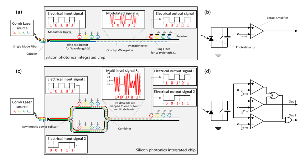
Network-on- chip (NoC) is a key component for boosting the system performance of future chip multiprocessors. With the projected increase in the number of cores on the chip, the NoC is perceived to be the limiting component for performance and scaling. Photonic NoCs are under serious consideration for scaling future multicore architectures. In this paper, we propose two photonic NoC architectures based on an optical multilevel signaling technique that can double the transmission bandwidth and reduce the area requirements. Simulation studies show that the proposed methodology saves up to 53% of power and reduces the area overhead by as much as 81% compared with metallic-based NoCs.
As throughput, scalability, and energy efficiency in network-on- chips (NoCs) are becoming critical, there is a growing impetus to explore emerging technologies for implementing NoCs in future multicore and many-core architectures. Two disruptive technologies on the horizon are nanophotonic interconnects (NIs) and 3D stacking. NIs can deliver high on-chip bandwidth while delivering low energy/bit, thereby providing a reasonable performance-per- watt in the future. Three-dimensional stacking can reduce the interconnect distance and increase the bandwidth density by incorporating multiple communication layers. In this paper, we propose an architecture that combines NIs and 3D stacking to design an energy-efficient and reconfigurable NoC.
We quantitatively compare the hardware complexity of the proposed topology to other nanophotonic networks in terms of hop count, network diameter, radix, and photonic parameters. To maximize performance, we also propose an efficient reconfiguration algorithm that dynamically reallocates channel bandwidth by adapting to traffic fluctuations. For 64-core reconfigured network, our simulation results indicate that the execution time can be reduced up to 25 percent for Splash-2, PARSEC, and SPEC CPU2006 benchmarks. Moreover, for a 256-core version of the proposed architecture, our simulation results indicate a throughput improvement of more than 25 percent and energy savings of 23 percent on synthetic traffic when compared to competitive on-chip electrical and optical networks.

Department of Electrical and Computer Enginnering
School of Engineering and Applied Science
The George Washington University
800 22nd Street NW
Washington, DC 20052
United States of America
Ahmed Louri, IEEE Life Fellow
David and Marilyn Karlgaard Endowed Chair Professor of ECE
Director, HPCAT Lab
Email: louri@gwu.edu
Phone: +1 (202) 994 8241

Drag and Drop Website Builder